 中
中
 0755-86529780
 中
中
 0755-86529780
The production of printed circuit boards (PCBs) involves a number of different processes, many of which require the use of lasers. Due to the ever-smaller apertures required, the use of UV nanosecond pulsed lasers is increasing.

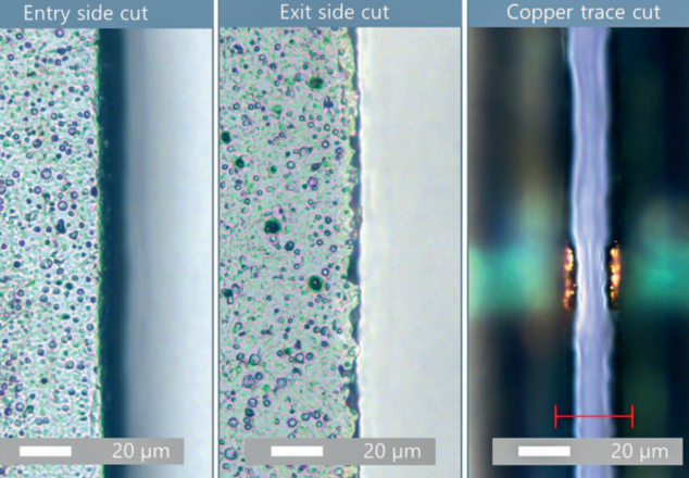
Figure 1. Optical microscope view of cuts through the entrance and exit surfaces of a 250 µm thick SiP material with embedded copper wires (net cutting speed 200 mm/s)
Devices and modules are becoming more compact thanks to advanced packaging techniques. Recognizing the large difference between semiconductor nodes and PCB dimensions (from nanometers to millimeters in extreme cases), developers continue to focus on developing advanced packaging technologies to connect components of different sizes. One of these technologies is the system-in-package (SiP) system, which bundles individual integrated circuit (IC) devices on a PCB substrate with embedded metal trace interconnects before final packaging and separation. This architecture typically includes an interposer to achieve a reasonable high-density chip connection distribution in the PCB. The final packaging is generally performed using epoxy molding compound (EMC) packaging or other methods, and the modules are still arranged on a single large panel during the final packaging. The modules are then separated using a laser cutting process.
Output, quality and cost must match
The ideal laser for SiP separation depends on the specific requirements and must strike the best balance between throughput, quality, and cost. When highly sensitive components are involved, it may be necessary to take advantage of ultrashort pulse (USP) lasers and/or the inherently low thermal effects of UV wavelengths. In other cases, lower cost, higher throughput nanosecond pulse and long-wave lasers are more appropriate choices. To demonstrate the high processing speeds for SiP PCB substrate cutting, MKS application engineers tested green high-power nanosecond pulse lasers. Using a Spectra-Physics Talon GR70 laser, SiP material consisting of thin FR4 with embedded copper wires and double-sided solder mask was cut using a high-speed multi-process technique with a dual-axis scanning galvanometer. The total material thickness is 250 µm, of which 150 µm is the (ultra-thin) FR4 board and the remaining 100 µm is the double-sided polymer solder mask. By using a high scanning speed of 6 m/s, severe thermal effects can be mitigated and the formation of a heat-affected zone (HAZ) can be avoided. Considering the relatively thin material, they used a small focal spot size (about 16 µm, 1/e2 diameter) and a high pulse repetition frequency (PRF) of 450 kHz. This combination of parameters can give full play to the laser's unique ability to maintain high power at high PRF (67 W at 450 kHz in this example), which helps to maintain appropriate energy density and spot-to-spot overlap at high scanning speeds.

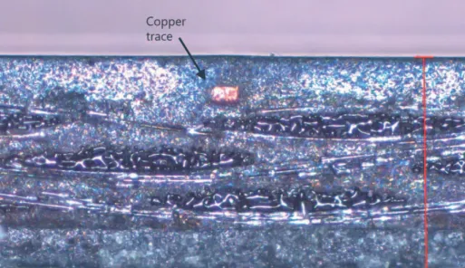
Figure 2. Side view of a laser-cut SiP showing excellent quality, especially inside the glass fabric and near the embedded copper wires
Cutting without thermal degradation
The overall net cutting speed achieved after multiple high-speed scans was 200 mm/s. Figure 1 shows the entrance and exit faces of the cut, as well as the subsurface area where the cut path intersects the buried copper wire. The cuts on both the entrance and exit faces are clean, with minimal or no HAZ. Furthermore, the presence of the copper wire did not adversely affect the cutting process, and the quality of the copper cut edge appears to be very good, despite the limited viewing angle.
For a more detailed look at the quality around the copper wire (and indeed the entire cut), a cross section of the cut sidewall can be viewed (Figure 2).
The quality is very good, with only minimal HAZ and a small amount of carbonization and particulate debris. Each fiber in the FR4 layer is clearly discernible, with melted portions limited to the cut fiber end faces protruding from the sidewall (i.e., perpendicular to the fibers running along the cut face). Importantly, no delamination is observed in these layers.
In addition, the results show that the area around the copper wire is of good quality, with no detrimental thermal effects, such as copper bleed or delamination from the surrounding FR4 or solder mask.
Thickened FR4 board with large spot diameter is required
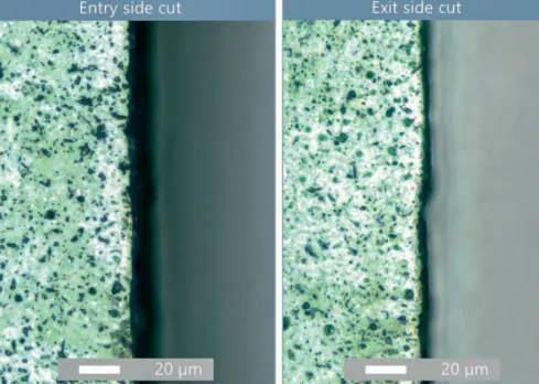
Cutting thick FR4 for device depaneling is a more established PCB application for nanosecond pulsed lasers, where small breakpoints are cut to separate array devices from the panel. The Talon GR70 was put to the test, and a new breakpoint cutting process was developed specifically for device panels consisting of approximately 900 µm thick FR4 boards. For this thicker material, using the largest possible focal spot diameter while maintaining sufficient energy density (in J/cm2) is critical to achieve good yields. Due to the laser's high pulse energy (>250 µJ) at a nominal PRF of 275 kHz, a larger spot size (approximately 36 µm) was used; in addition, the beam quality is very good, with a Rayleigh range of more than 1.5 mm for the focused beam, which is 1.5 times the material thickness. As a result, the spot size is relatively large and constant throughout the thickness of the material, which helps achieve efficient cutting because the uniform irradiation volume and the resulting wide grooves facilitate debris evacuation. Figure 3 shows the entrance and exit micrographs of a cut machined using multiple high-speed scans at 6 m/s (overall net cutting speed of 20 mm/s).

Figure 3. FR4 PCB (900 µm thick) incident and exit surfaces after laser cutting at a net cutting speed of 20 mm/s
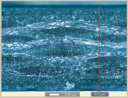
Similar to the case of the SiP board, the surface quality on both the entrance and exit sides of the cut is very good, and the resulting HAZ is minimal. Due to the non-uniform properties of the glass/epoxy FR4 substrate and the lower energy density at the far end of the laser ablation cut, the exit cut edge will generally deviate slightly from a perfect straight line. Cross-sectional sidewall imaging shows more details about the cut quality (Figure 4 below).

Figure 4. Laser-cut sidewall view of FR4 (900 μm thick), showing excellent quality. Carbonization is very low to zero, and the fiber bundles are almost not melted.
In Figure 4 we can see that excellent quality is achieved. Only a small amount of HAZ and carbon products (char) are formed at the cut. Also, almost no melting of the glass fibers occurs. With a net cutting speed of up to 20 mm/s, the Talon GR70 is clearly well suited for depaneling thicker FR4 PCBs while ensuring excellent quality and high throughput.